
Scaling Dual Active Bridge Transformers for Medium-Voltage Applications.

PDF Version

Introduction
The transition toward Medium-Voltage (MV) Solid-State Transformers (SST) is driven by the need for higher efficiency and smaller footprints in data centers and electric vehicle charging infrastructure. At the heart of these systems is the Medium-Frequency Transformer (MFT), which serves as the critical galvanic isolation barrier. Scaling these components for megawatt-level applications requires moving beyond traditional insulation designs to address long-term reliability under extreme common-mode (CM) voltage and high dv/dt stress. This whitepaper details a modular design approach using an IsoGap Transformer architecture to achieve high power density and reliable, partial-discharge-free operation at 35 kV.
The Motivation for Medium-Voltage Scaling
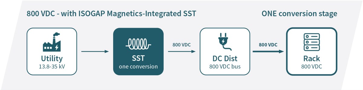
Current power architectures are evolving to meet the demands of next-generation 800V servers and high-power charging stations. Compared to traditional low-voltage solutions, a 1MW SST can achieve a 2x reduction in volume, a 3x reduction in mass, and a 2.5x reduction in the required concrete pad footprint while increasing efficiency from 92% to 96%. Future medium-voltage rectification applications, such as 800 VDC data center distribution, will require systems at multi-megawatt power levels. Building these from a practical number of modules requires the Dual Active Bridge (DAB) kernel to scale from current 55 kW designs to 60-250 kW per module, with input voltages reaching +/- 6500 V and switching frequencies up to 100 kHz.
Technical Challenges: Beyond Dielectric Withstand
Standard insulation design is typically “withstand-based,” validated by High-Potential (Hi-Pot) and Basic Insulation Level (BIL) tests. While these confirm short-term dielectric strength, they fail to capture the long-term degradation mechanisms prevalent in high-frequency MV environments.
Partial Discharge (PD) as the Real Limit: The true operating limit is defined by the Partial Discharge Inception Voltage (PDIV). PDIV often occurs well below the breakdown voltage, especially under CM stress. Repetitive PD causes localized heating and material erosion, leading to unpredictable, progressive failures.
Dominant Electrical Stress: In cascaded MV architectures, common-mode stress between windings dominates, with peak potentials potentially reaching 50 kV. Differential-mode transients further couple into this stress via parasitic capacitances.
Design Philosophy: The IsoGap Transformer
To scale DAB transformers reliably, an IsoGap Transformer concept that physically separates the transformer into distinct High-Voltage (HV) and Low-Voltage (LV) zones is recommended.
Key Architectural Features include:
Electric-Field Control: Instead of simply increasing insulation thickness—which penalizes size, weight, and magnetic coupling—designers use semiconductive field-grading layers. This optimizes geometry to confine the E-field and minimizes stress at “triple-point” locations where different materials meet.
Potential Management: To avoid uncontrolled field distribution, the isolation structure references key components, such as the ferrite core, to a controlled potential rather than allowing them to float.
Surface Discharge Mitigation: Creepage distances are extended geometrically to control tangential E-field components that drive tracking and surface discharge.
Minimizing Parasitics: Designers minimize the primary-to-secondary capacitance and control the path of 60Hz and high frequency current provided by CM voltage through the use of semiconductive shields. Limiting this capacitance is vital for reducing CM current and Electromagnetic Interference (EMI).
Validation and Results
The scalability of this modular approach has been demonstrated through several prototypes:
15 kV Class SST: Twenty samples were integrated into a field-deployed SST, consistently passing PDIV tests at a mean of 17.8 kVrms.
High-Density Design: An optimized air-cooled design achieved a power density of 15 kW/L at 80 kW.
High-Insulation Design: A specialized design achieves a 35 kV PDIV rating while maintaining a 0.98 coupling coefficient.
Conclusion
Scaling Dual Active Bridge transformers for medium-voltage applications requires a fundamental shift toward PD-free design and sophisticated electric-field shaping. By utilizing a two-zone isolation structure with field grading and controlled core potentials, manufacturers can produce modular, compact MFTs that provide the long-term reliability necessary for the next generation of power grid infrastructure.

Additional Appendixes
1. What are semiconductor field-grading layers?
In the context of scaling medium-voltage transformers, semiconductive field-grading layers are specialized materials used within an isolation structure to manage and redistribute electric field stress.
They serve several critical functions in the design of high-power components like the IsoGap Transformer:
Mitigating E-Field Hotspots: Sharp edges and material interfaces often create localized electric field concentrations (“hotspots”) that can trigger Partial Discharge (PD). Field-grading layers utilize optimized geometry and specific material selection to confine the electric field away from these vulnerable areas.
Triple-Point Control: These layers help control the “triple-point” locations—the areas where air, solid insulation, and a conductor meet. By managing these points, designers can minimize field intensity in the air, thereby increasing the Partial Discharge Inception Voltage (PDIV).
Alternative to Bulky Insulation: A traditional approach to preventing discharge is simply increasing the thickness of the insulation. However, this adds significant size and weight while reducing magnetic coupling. Field grading offers a “field shaping” alternative that allows for compact, high-density designs (up to 15 kW/L) without compromising long-term reliability.
Potential Management: In the proposed modular architectures, these layers work in tandem with controlled potential referencing to ensure that conductive components, such as the ferrite core, do not float, which would otherwise increase uncontrolled electric-field stress.
By using these layers, it is possible to achieve reliable, PD-free operation under common-mode voltages of 35 kV while maintaining a scalable and thermally efficient transformer footprint.

2. Air-cooled vs. Liquid-cooled design efficiencies
As commonly understood, transitioning from air-cooled to liquid-cooled designs in medium-voltage power systems results in significant efficiency improvements at both the component and system levels:
Data Center System Gains: Liquid cooling removes heat far more effectively than air, cutting the fan and chiller energy needed for thermal management. In data center applications, this is projected to deliver system-level efficiency gains of up to 27% by 2030.
Scalability Requirements: While current 55 kW Dual Active Bridge (DAB) kernels utilize forced air cooling, future designs aiming for 60–250 kW per module are identified as requiring liquid cooling to handle the increased power density and thermal demands.
Architectural Compatibility: The proposed IsoGap Transformer is specifically noted for being thermally efficient and highly compatible with liquid cooling systems, which supports its ability to scale to higher power levels.
In summary, liquid-cooled designs are essential for achieving the higher power density required for next-generation 800V server environments and megawatt-scale power delivery infrastructure.

ABOUT THE AUTHOR: Nicola Rosano is an Engineering Manager at Standex Electronics, where he works on planar magnetics, resonant converters, and Configure-to-Order (CTO) solutions. He has designed power electronics for spacecraft, for electric vehicles, and for automotive customers. He is co-author of Power Supplies A to Z, 3rd edition, and holds patent filings in EV and wireless power conversion.
ABOUT THE INVENTOR OF ISOGAP ISOLATION TRANSFORMER TECHNOLOGY: Srdjan Lukic is a Lampe Distinguished Professor of Electrical & Computer Engineering at NC State University and has 20+ years in power electronics and high-frequency magnetics for solid-state transformers (SSTs). He led the development of SSTs at NC State and recently demonstrated system operation in the field with the Electric Power Research Institue (EPRI) and the New York Power Authority (NYPA).
Related Articles
-

Powering the Digital Frontier
How Standex Edge enables the Next Generation of Computing with High-Performance Power Magnetics.
-

Optimizing Motor Performance
How Custom Standex Edge Magnetics Maximized the Flexibility and Scalability of a Motor Manufacturer’s Motion Solutions.
-

Planar Transformers
How to Select Planar Magnetics for Low Profile, High Reliability Industrial System Designs
-

Smart Grid Thermal Management
How Temperature Managing Magnetics Improve Efficiency, Reliability, and Power Density in Smart Grid Systems